Chip Fit
Location:
TestBenches / AraTestBenches / ChipFit / (several available)
This test bench is designed to estimate whether the components in your design will fit within a given circuit board area. Given the footprints of the individual components, it will try to find an arrangement that accommodates all parts. It will then report as to whether or not the elements can fit within the given area.
Note: The Chip Fit analysis should be used only to confirm that the selected components will not fit within the given area. A completed design will require more area for signal traces and other considerations. Consider a “no” answer definitive but a “yes” answer to require further investigation.
Test benches are provided for these Ara module sizes: - Front H - Front I - Rear 1x1 - Rear 1x2 - Rear 2x2
Consult the Ara MDK for details on each size.
Configure
First, you’ll need to create a copy of one of the Chipfit test benches. For instructions, refer to the section Project Ara Test Bench Basics.
No additional configuration is needed to test a design against one of
the standard Ara sizes provided. However, if you would like to test for
a different size, change the boardHeight and boardWidth
Parameters accordingly.
Metrics
Note: In the Metric names that follow, (x) and (y) are replaced by the boardWidth and boardHeight, respectively, as defined above.
| Name | Value Type | Description |
|---|---|---|
| fits_(x)_by_(y) | true/false | Whether the components in the design will fit within the given space |
| pct_occupied_(x)_by_(y) | real number | The percentage of the available space occupied by the given components. |
Outputs
| Filename | Description |
|---|---|
showChipFitResults.bat |
Launches a visualizer for the Chip Fit results. |
Chip Fit Visualizer
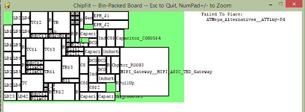
Running showChipFitResults.bat in the results folder will launch the
Chip Fit Visualizer. This utility will show the best-case packing of
the design’s elements.
If any elements failed to pack into the given area, their names will be listed under the Failed To Place heading at the right side of the diagram.

Chip Fit Visualizer
The Chip Fit Visualizer has the following controls:
- Numpad + key: zoom in
- Numpad - key: zoom out
- Esc: quit
Assumptions
This analysis assumes that each component to be placed on the printed circuit board (PCB) has an EDA Model (EAGLE Schematic file) associated with it. Information about each component’s size is taken from that model file.